Thursday 31 January 2008

COMP 372 Assgn. # 5 Internal Circuit of 6810 Microprocessor

The MCM6810, a 128 x 8 chip designed by Motorola is used with its 6800 series processors. This means it stores 128 bytes at addresses from $00 to $7F. If you put any address on the 7 address pins, then the corresponding data appears on the 8 data pins. The time from a change of address to the appearance of the corresponding data is called the access time of the memory. Actually, it is the maximum access time, since each address has, in general, a different access time depending on where it is in the memory array. An access time of 450 ns was appropriate to processors with a 1 μs cycle time, assuming that the proper address would appear midway in the cycle, and the data would be read or written at the end of the cycle.

Since the data pins are connected to the processor's data bus, they must be put into a high-impedance state at all times except when the processor expects them to drive the bus during a read cycle. There are two control lines for the memory chip, the chip select (CS) and the read-write (RW) lines. When RW is high, data appears when CS is active. The 6810 has six CS pins, four active low and two active high. All must be active to say that CS is active.

When RW is low, CS has a different function. Instead of activating the data outputs, it strobes the data on the data bus into the current address on the trailing edge of its pulse. Different memory chips may work in different ways, but something like this occurs in any case. This happens to be the way the 6810 works.

When the 6810 is connected to the processor in the normal way, the RW line is connected to the R/W signal of the processor, which takes its proper value at the start of the cycle. CS is active during φ2, which is the clock signal produced by the processor that is high during the last half of the bus cycle. If the 6810 were the only thing on the bus (and it will be for our initial test) one can simply use φ2 as CS. In a more general case, CS will combine both φ2 and an address decode depending on the current address output by the processor. Different devices on the bus will have different address decodes.


The Internal Structure


References

http://mysite.du.edu/~jcalvert/tech/6504.htm

http://www.datasheetarchive.com/preview/441555.html

COMP 372 Assgn. # 4 Role Of Microprocessor in Computer

The simplified model of a microprocessor consists of five parts, which are:

Arithmetic & Logic Unit (ALU)
The part of the central processing unit that deals with operations such as addition, subtraction, and multiplication of integers and Boolean operations. It receives control signals from the control unit telling it to carry out these operations. For more, click the title above.

Control Unit (CU)
This controls the movement of instructions in and out of the processor, and also controls the operation of the ALU. It consists of a decoder, control logic circuits, and a clock to ensure everything happens at the correct time. It is also responsible for performing the instruction execution cycle. More on the control unit can be discovered by clicking the title above.

Register Array
This is a small amount of internal memory that is used for the quick storage and retreival of data and instructions. All processors include some common registers used for specific functions, namely the program counter, instruction register, accumulator, memory address register and stack pointer. For more, click the title above.

System Bus
This is comprised of the control bus, data bus and address bus. It is used for connections between the processor, memory and peripherals, and transferal of data between the various parts. Click the title above for more.

Memory
The memory is not an actual part of the CPU itself, and is instead housed elsewhere on the motherboard. However, it is here that the program being executed is stored, and as such is a crucial part of the overall structure involved in program execution.


The ALU, or the arithmetic and logic unit, is the section of the processor that is involved with executing operations of an arithmetic or logical nature. It works in conjunction with the register array for many of these, in particular, the accumulator and flag registers. The accumulator holds the results of operations, while the flag register contains a number of individual bits that are used to store information about the last operation carried out by the ALU. More on these registers can be found in the register array section.

The control unit is arguably the most complicated part of this model CPU, and is responsible for controlling much of the operation of the rest of the processor. It does this by issuing control signals to the other areas of the processor, instructing them on what should be performed next.

A register is a memory location within the CPU itself, designed to be quickly accessed for purposes of fast data retrieval. Processors normally contain a register array, which houses many such registers. These contain instructions, data and other values that may need to be quickly accessed during the execution of a program.

The system bus is a cable which carries data communication between the major components of the computer, including the microprocessor.

Reference
http://www.eastaughs.fsnet.co.uk/cpu/structure-bus.htm

Wednesday 30 January 2008

COMP 372 Assgn. # 3 Different ROM and RAM IC's

ROM - Read-only memory: On ROM, data is prerecorded for read only which can not be removed. ROM is nonvolatile and it retains its contents regardless the computer is on or off.

RAM - Random access memory: whose contents can be accessed (read, write and remove) in any order. This is in contrast to sequential memory devices such as magnetic tapes, discs and drums, in which the mechanical movement of the storage medium forces the computer to access data in a fixed order. RAM is usually used for primary storage in computers to hold active information such as data and programs. Common forms of RAM are: SRAM (Static RAM) and DRAM (Dynamic RAM).

There are also some hybrad memory types which combines characters of both RAM and ROM, such as Flash memory, NVRAM and EEPROM.

Type Volatile Writeable Erase Size Max Erase Cycles Speed
SRAM Yes Yes Byte Unlimited Fast
DRAM Yes Yes Byte Unlimited Moderate
Masked ROM No No n/a n/a Fast
PROM No Once, with a device programmer n/a n/a Fast
EPROM No Yes, with a device programmer Entire Chip Limited
Fast
EEPROM No Yes Byte Limited
Fast to read, slow to erase/write
Flash No Yes Sector Limited
Fast to read, slow to erase/write
NVRAM No Yes Byte Unlimited Fast

Computer Memory: RAM and ROM

Computer Memory: RAM and ROM

Related Terms:RAM, ROM, Flash memory, DRAM, SRAM


References

http://www.networkdictionary.com/hardware/cm.php

http://www.arcadecomponents.com/catalog/item/2251646/1693323.htm#image_1


Monday 28 January 2008

COMP 372 Assgn. # 2 Different IC numbers & Layout for Decorders,Encorders & Multiplexers

IC Numbers (For Decorders)

SN54246
SN544247
SN54LS247
SN64LS248
SN74246
SN74247
SN74LS24


Ic Numbers For Encorders

MM54C922-16 Key Encorder
MM74C922-16 Key Encorder
MM54c923-20 Key Encorder
MM74C923-20 Key Encorder


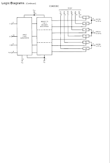
Block Diagram


Ic Numbers For Multiplexers

CD 4051BC Single 8 Channel Analog Multiplexer
CD4052BC
Single 8 Channel Analog Multiplexer
CD4053BC Single 8 Channel Analog Multiplexer


Reference
http://www.nalanda.nitc.ac.in/industry/appnotes/TI_logic/data/www.ti.com/sc/psheets/sdls083/sdls083.pdf

http://eshop.engineering.uiowa.edu/NI/pdfs/00/60/DS006037.pdf
http://www.ic-on-line.cn/IOL/viewpdf/CD4053_10260.htm

COMP 372 Assgn. # 1 IC Layout for 6800 family

The 68000 has eight 32-bit data registers (D0-D7), eight 32-bit address registers (A0-A7), a 32-bit program counter, two 32-bit stack pointers, and a 16-bit status register (Figure 7-1). The processor is capable of handling data as either 32-bit-long words, 16-bit words, bytes, or bits.
N.B CLICK AN IMAGE FOR AN EXPANDED VIEW

Figure 7-1: Programmer's model of the 68000
The processor has two modes of operation, supervisor mode (operating system) and user mode (applications). The mode of operation is made available to external hardware, thereby allowing the address decoder to have separate supervisor and user spaces.
Figure 7-2: MC68000 block diagram and pinout


Reference
www.datasheetarchive.com/search.php?t=0&q=6800+&manystr=&sub.x=0&sub.y=0