Thursday 29 November 2007

RF ASSGN # 10 SATELLITE COMMUNICATION


In order for any communication satellite to function, it must have :
A receiver and receiver antenna, to be able to receive information from the originating ground station via the uplink.
A transmitter and transmitter antenna to be able to relay the information from the satellite to the destination groundstation via the downlink.
A method for connecting the uplink and the downlink for retransmitting.
A prime electrical power to run all the electronics
Click HERE to view the major satellites in Kenya mostly for the local TV stations
The exact nature of these components will differ, depending on the orbit and the system architecture, but every communication satellite must have these basic components.
Reference

Monday 19 November 2007

CMMT ASSGN # 9 Different kinds of antenna, their function, matching and application


Application

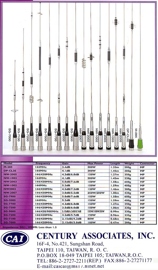
SMA & optical fiber connectors, RF coaxial connectors, antennas for ham radios & cellular phones, RF linear amplifiers & boosters, cable assemblies, & metal products


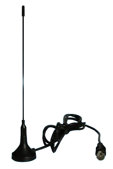
ANTENNA 2


Frequency Range VHF 174-230 / UHF 470-862MHz

Input Impedance 50 Ohm / 75 Ohm
Gain 3.5dBi

VSWR <1.5>


Antenna 3


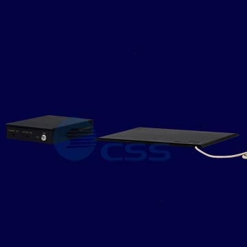
RF 8.2MHz system

Specifications:
1) Stainless steel pipe, top ABS housing
2) Detection range: 1.3- 1.8m
3) Dimensions: 32 x 168cm
4) Center frequency: 8.2MHz±0.5MHz
5) Scanning frequency bias: ±500kHz
6) Scan rate: four optional
7) Sensitivity: 5μA
8) Bandwidth: 7.7 - 8.7MHz
9) Safe gu ard: 250V , 0.5A, fuse self-remedy


Antenna 4


Description:


- Frequency: 7.7- 8.7MHz

- Deactivating height: up to 20CM

- Deactivating speed: 160pcs/m

- Power consumption: ≤6W


Antenna 5


Features:

1)Dimension: 25*70mm

2)Frequency: 8.2MHz/58KHz

3)Color: black/white/grey or customize

4)loose Lock: Three balls clutch,standard/super

5)Detection Range: 1.3 m-2.8m (5.1'-11')

Reference
http://shanghaielson.en.alibaba.com/product/50072805/200476204/EAS_AM_SECURITY_HARD_TAG/EAS_AM_LARGE_PENCIL_TAG_B.html

CMMT 390 ASSGN # 8 Amplifier Classes of Operation and Biasing Networks.

Amplifier classes

Amplifier circuits are classified as A, B, AB and C for analog designs, and class D and E for switching designs. For the analog classes, each class defines what proportion of the input signal cycle (called the angle of flow) is used to actually switch on the amplifying device:

Class A
100% of the input signal is used (conduction angle a = 360° or 2π)
Class AB
more than 50% but less than 100% is used. (181° to 359°, π <>
  • Class AB1 applies to tube or transistor amplifiers in class AB where the grid or base is more negatively biased than it is in class A.
  • Class AB2 applies to tube or transistor amplifiers in class AB where the grid or base is often more negatively biased than in AB1, and the input signal is often larger. When the drive is high enough to make the grid or the base more positive, the grid or base current will increase. It is possible depending on the level of the signal input for the amplifier to move from class AB1 to AB2.
Class B
50% of the input signal is used (a = 180° or π)
Class C
less than 50% is used (0° to 179°, a < π)

This can be most easily understood using the diagrams in each section below. For the sake of illustration, a bipolar junction transistor is shown as the amplifying device, but in practice this could be a MOSFET or vacuum tube device. In an analog amplifier (the most common kind), the signal is applied to the input terminal of the device (base, gate or grid), and this causes a proportional output drive current to flow out of the output terminal. The output drive current comes from the power supply.

The voltage signal shown is thus a larger version of the input, but has been changed in sign (inverted) by the amplification. Other arrangements of amplifying device are possible, but that given (that is, common emitter, common source or common cathode) is the easiest to understand and employ in practice. If the amplifying element is linear, then the output will be faithful copy of the input, only larger and inverted. In actual practice, transistors are not linear, and the output will only approximate the input. Non-linearity from any of several sources is the origin of distortion within an amplifier. Which class of amplifier (A, B, AB or C) depends on how the amplifying device is biased — in the diagrams the bias circuits are omitted for clarity.

Any real amplifier is an imperfect realisation of an ideal amplifier. One important limitation of a real amplifier is that the output it can generate is ultimately limited by the power available from the power supply. An amplifier will saturate and clip the output if the input signal becomes too large for the amplifier to reproduce or if operational limits for a device are exceeded.

Class A

Advantage

Class A amplifying devices operate over the whole of the input cycle such that the output signal is an exact scaled-up replica of the input with no clipping. Class A amplifiers are the usual means of implementing small-signal amplifiers. They are not very efficient; a theoretical maximum of 50% is obtainable with inductive output coupling and only 25% with capacitive coupling.

Disadvantage

In a Class A circuit, the amplifying element is biased so the device is always conducting to some extent, and is operated over the most linear portion of its characteristic curve (known as its transfer characteristic or transconductance curve). Because the device is always conducting, even if there is no input at all, power is drawn for the power supply. This is the chief reason for its inefficiency.

Image:Electronic Amplifier Class A.png
Class A Amplifier

If high output powers are needed from a Class A circuit, the power waste (and the accompanying heat) will become significant. For every watt delivered to the load, the amplifier itself will, at best, dissipate another watt. For large powers. this means very large and expensive power supplies and heat sinking. Class A designs have largely been superseded for audio power amplifiers, though some audiophiles believe that Class A gives the best sound quality, due to it being operated in as linear a manner as possible which provides a small market for expensive high fidelity Class A amps. In addition, some aficionados prefer thermionic valve (or "tube") designs instead of transistors, for several claimed reasons:

tubes are more commonly used in class A designs, which have an asymmetrical transfer function. This means that distortion of a sine wave creates both odd- and even-numbered harmonics. The claim is that this sounds more "musical" than the higher level of odd harmonics produced by a symmetrical push-pull amplifier.[1][2] Though good amplifier design can reduce harmonic distortion patterns to almost nothing, the increase in distortion in some amplifier designs is essential to the sound of intentional electric guitar distortion.

Another is that valves use many more electrons at once than a transistor, and so statistical effects lead to a "smoother" approximation of the true waveform — see shot noise for more on this. Junction field-effect transistors (JFETs) have similar characteristics to valves, so these are found more often in high quality amplifiers than bipolar transistors. Historically, valve amplifiers often used a Class A power amplifier simply because valves are large and expensive; many Class A designs uses only a single device.

Transistors are much cheaper, and so more elaborate designs that give greater efficiency but use more parts are still cost effective. A classic application for a pair of class A devices is the long-tailed pair, which is exceptionally linear, and forms the basis of many more complex circuits, including many audio amplifiers and almost all op-amps. Class A amplifiers are not often used in output stages of op-amps; they are sometimes used as medium-power, low-efficiency, and high-cost audio amplifiers. The power consumption is unrelated to the output power. At idle (no input), the power consumption is essentially the same as at high output volume. The result is low efficiency and high heat dissipation.

Class B and AB

Class B amplifiers only amplify half of the input wave cycle. As such they create a large amount of distortion, but their efficiency is greatly improved and is much better than Class A. Class B has a maximum theoretical efficiency of 78.5%. This is because the amplifying element is switched off altogether half of the time, and so cannot dissipate power. A single Class B element is rarely found in practice, though it can be used in RF power amplifiers where the distortion levels are less important. However Class C is more commonly used for this.

Image:Electronic Amplifier Class B fixed.png
Class B Amplifier

A practical circuit using Class B elements is the complementary pair or "push-pull" arrangement. Here, complementary or quasi-complementary devices are used to each amplify the opposite halves of the input signal, which is then recombined at the output.

Disadvantage

This arrangement gives excellent efficiency, but can suffer from the drawback that there is a small mismatch at the "joins" between the two halves of the signal. This is called crossover distortion. A solution to this is to bias the devices to be just on, rather than completely off when they're not in use. This is called Class AB operation.

Each device is operated in a non-linear region which is only linear over half the waveform, but still conducts a small amount on the other half. Such a circuit behaves as a class A amplifier in the region where both devices are in the linear region, however the circuit cannot strictly be called class A if the signal passes outside this region, since beyond that point only one of the devices will remain in its linear region and the transients typical of class B operation will occur. The result is that when the two halves are combined, the crossover is greatly minimised or eliminated altogether.

Advantage

Class AB sacrifices some efficiency over class B in favor of linearity, so will always be less efficient. (below 78.5%) It is typically much more efficient than class A.

Image:Electronic Amplifier Push-pull.png
Class B Push-Pull Amplifier

Class B or AB push-pull circuits are the most common design type found in audio power amplifiers. Class AB is widely considered a good compromise for audio amplifiers, since much of the time the music is quiet enough that the signal stays in the "class A" region, where it is amplified with good fidelity, and by definition if passing out of this region, is large enough that the distortion products typical of class B are relatively small. The crossover distortion can be reduced further by using negative feedback. Class B and AB amplifiers are sometimes used for RF linear amplifiers as well. Class B amplifiers are also favored in battery-operated devices, such as transistor radios.

Digital Class B

A limited power output Class-B amplifier with a single-ended supply rail of 5V +/- 10%.

Class C

Class C amplifiers conduct less than 50% of the input signal and the distortion at the output is high, but high efficiencies (up to 90%) are possible. Some applications (for example, megaphones) can tolerate the distortion. A much more common application for Class C amplifiers is in RF transmitters, where the distortion can be vastly reduced by using tuned loads on the amplifier stage. The input signal is used to roughly switch the amplifying device on and off, which causes pulses of current to flow through a tuned circuit.

The tuned circuit will only resonate at particular frequencies, and so the unwanted frequencies are dramatically suppressed, and the wanted full signal (sine wave) will be abstracted by the tuned load. Provided the transmitter is not required to operate over a very wide band of frequencies, this arrangement works extremely well. Other residual harmonics can be removed using a filter.

Image:Electronic Amplifier Class C.png
Class C Amplifier

Class D

Class D amplifiers are much more efficient than Class AB power amplifiers. As such, Class D amplifiers do not need large transformers and heavy heatsinks, which means that they are smaller and lighter in weight than an equivalent Class AB amplifier. All power devices in a Class D amplifier are operated in on/off mode. Output stages such as those used in pulse generators are examples of class D amplifiers. The term usually applies to devices intended to reproduce signals with a bandwidth well below the switching frequency.


These amplifiers use pulse width modulation, pulse density modulation (sometimes referred to as pulse frequency modulation) or more advanced form of modulation such as Delta-sigma modulation (for example, in the Analog Devices AD1990 Class-D audio power amplifier).

The input signal is converted to a sequence of pulses whose averaged value is directly proportional to the instantaneous amplitude of the signal. The frequency of the pulses is typically ten or more times the highest frequency of interest in the input signal. The output of such an amplifier contains unwanted spectral components (that is, the pulse frequency and its harmonics) which must be removed by a passive filter. The resulting filtered signal is then an amplified replica of the input.

Advantage

The main advantage of a class D amplifier is power efficiency. Because the output pulses have a fixed amplitude, the switching elements (usually MOSFETs, but valves and bipolar transistors were once used) are switched either on or off, rather than operated in linear mode. This means that very little power is dissipated by the transistors, except during the very short interval between the on and off states. The wasted power is low because the instantaneous power dissipated in the transistor is the product of voltage and current, and one or the other is almost always close to zero. The lower losses permit the use of a smaller heat sink while the power supply requirements are lessened too.

Class D amplifiers can be controlled by either analog or digital circuits. The digital control introduces additional distortion called quantization error caused by its conversion of the input signal to a digital value.

Class D amplifiers have been widely used to control motors, and almost exclusively for small DC motors, but they are now also used as audio amplifiers, with some extra circuitry to allow analogue to be converted to a much higher frequency pulse width modulated signal. The relative difficulty of achieving good audio quality means that nearly all are used in applications where quality is not a factor, such as modestly-priced bookshelf audio systems and "DVD-receivers" in mid-price home theater systems.

Disadvantage

The drawback with Class D designs being used to power subwoofers is that their output filters (typically inductors that convert the pulse width signal back into an analogue waveform) lower the damping factor of the amplifier.

This means that the amplifier cannot prevent the subwoofer's reactive nature from lessening the impact of low bass sounds (as explained in the feedback part of the Class AB section). Class D amplifiers for driving subwoofers are relatively inexpensive, in comparison to Class AB amplifiers. A 1000 watt Class D subwoofer amplifier that can operate at about 80% to 95% efficiency costs about $250 USD, much less than a Class AB amplifier of this power, which would cost several thousand dollars.

The letter D used to designate this amplifier class is simply the next letter after C, and does not stand for digital. Class D and Class E amplifiers are sometimes mistakenly described as "digital" because the output waveform superficially resembles a pulse-train of digital symbols, but a Class D amplifier merely converts an input waveform into a continuously pulse-width modulated (square wave) analog signal. (A digital waveform would be pulse-code modulated.)


Types of Amplifier Biasing Networks.

Bipolar Transistor Biasing Networks.

Field Effect Transistor Biasing Networks.

single-Stub Matching Networks.

Double-Stub Matching Networks.

Reference

http://en.wikipedia.org/wiki/Operational_amplifier

COMP 362 ASSGN # 10 Digital to Analog conversion circuits with their specific functions

The following circuit, derived from the DAC0832 digital to analog converter (DAC) datasheet is one approach to making the conversion from stepwise digital information to a voltage. It's called an R 2R ladder and is part of the circuit used in the two DAC0832s on the board. R and Rfb are about 15K ohms, which makes 2R about 30K ohms. The actual values are not as important as the fact that the resistors are very closely matched to each other.

The "1" and "0" indicate the positions of MOSFET switches in the converter. A switch will connect to the "1" side if the corresponding bit is on, and to the "0" side if the bit is off. A switch connected to the "1" position will send a portion of Vref-derived current to Iout1, whereas a switch connected to the "0" position will send a portion of the current to Iout2.


To see how the R 2R ladder fits into the scheme of things, consider the following. The left side is a copy of one of the DAC0832 sections taken from the board's schematic. On the right is a simplified block diagram of the same thing, derived from the datasheet. Rfb is drawn in the manner shown to indicate it is internal to the DAC but can be accessed outside and be connected the Op-Amp:


Iout1 of the R 2R ladder is connected to the inverting input of the Op-Amp for more on Op-Amps). Iout2 of the R 2R ladder is connected to the non-inverting input and to ground. One end of the internal Rfb feedback resistor is connected to the output of the external Op-Amp. The other end is internally connected to the R 2R ladder's Iout1 as shown above. Thus, it is connected from the output of the Op-Amp to the inverting input.


CIRCUIT # 2


The current through R1 does not influence the current referenced at the inverting input. Although one end is connected to the -5V reference, the other end simply goes to ground, so the current through R1 never even makes it to the inverting input.

All of the other resistors do contribute to the current at the inverting input and to the output of the amplifier. The current through R2 splits into two paths. One is through R3 which goes directly to the inverting input, and the other is through the network of R4 and all of the other resistors to ground. The method to determine their composite value is more easily seen if the R4 part of the drawing is reorganized. A careful study will show that only the drawing has changed. The circuit is the same:


First consider the two 30K resistors on the bottom. Recalling the parallel resistor equation from How To Read A Schematic,
Rparallel = 1/(1/30K + 1/30K) = 15K ohms

A tip: the parallel value of resistors of the same value is the value of one of the resistors divided by the number of resistors.

The 15K parallel combination adds to the 15K above it since it is in series with it. Again, from How To Read A Schematic,
Rseries = 15K + 15K = 30K ohms

This 30K combination is in parallel with the 30K to the left of it, which produces 15K again which adds to the 15K above to produce 30K, and so on. The final value of the network is 30K. It would be a very good idea to print the picture, calculate the values and write them down as an exercise to clarify the process. There are other, more sophisticated ways to analyze the circuit, but this is straight forward and will do just fine for now.

Reference

http://www.learn-c.com/experiment8.htm


COMP 362 ASSGN # 9 Analog to Digital conversion circuits And Functions


FUNCTION
The circuit of A-to-D converter shown here is configured around ADC 0808, avoiding the use of a microprocessor. The ADC 0808 is an 8-bit A-to-D converter, having data lines D0-D7. It works on the principle of successive approximation. It has a total of eight analogue input channels, out of which any one can be selected using address lines A, B and C. Here, in this case, input channel IN0 is selected by grounding A, B and C address lines.

Usually the control signals EOC (end of conversion), SC (start conversion), ALE (address latch enable) and OE (output enable) are interfaced by means of a microprocessor. However, the circuit shown here is built to operate in its continuous mode without using any microprocessor. Therefore the input control signals ALE and OE, being active-high, are tied to Vcc (+5 volts). The input control signal SC, being active-low, initiates start of conversion at falling edge of the pulse, whereas the output signal EOC becomes high after completion of digitisation. This EOC output is coupled to SC input, where falling edge of EOC output acts as SC input to direct the ADC to start the conversion.

As the conversion starts, EOC signal goes high. At next clock pulse EOC output again goes low, and hence SC is enabled to start the next conversion. Thus, it provides continuous 8-bit digital output corresponding to instantaneous value of analogue input. The maximum level of analogue input voltage should be appropriately scaled down below positive reference (+5V) level.

The ADC 0808 IC requires clock signal of typically 550 kHz, which can be easily derived from an astable multivibrator constructed using 7404 inverter gates. In order to visualise the digital output, the row of eight LEDs (LED1 through LED8) have been used, wherein each LED is connected to respective data lines D0 through D7. Since ADC works in the continuous mode, it displays digital output as soon as analogue input is applied. The decimal equivalent digital output value D for a given analogue input voltage Vin can be calculated from the relationship


Reference
http://www.electronic-circuits-diagrams.com/computersimages/computersckt2.shtml

COMP 362 ASSGN # 7 DIGITAL IC DECODER AND ENCODER

IC NO.

FUNCTION

SPECIFICATION

7441

BCD to Decimal Decoder

NIXIE Tube Driver

7442

BCD to Decimal Decoder

7443

Excess-3 to Decimal Decoder

7444

Excess-3-Gray to Decimal Decoder

7445

BCD to Decimal Decoder/Driver

7446

BCD to 7-segment Decoder/Driver

15V Open Collector Outputs30V Open Collector Outputs

7447

BCD to 7-segment Decoder/Driver

7448

BCD to 7-segment Decoder/Driver

7449

BCD to 7-segment Decoder/Driver

Open Collector Outputs

74137

3 to 8-line Decoder/Demultiplexer with Address Latch

74138

3 to 8-line Decoder/Demultiplexer

74139

Dual 2 to 4-line Decoder/Demultiplexer

74140

Dual 4-input NAND Line Driver

74141

BCD to Decimal Decoder/Nixie Tube Driver

74142

Decade Counter/Latch/Decoder

Nixie Tube Driver

74143

Decade Counter/Latch/Decoder/7-segment Driver

15 mA Constant Current

74144

Decade Counter/Latch/Decoder/7-segment Driver

15V Open Collector

74145

BCD to Decimal Decoder/Driver

74147

10-Line to 4-Line Priority Encoder

74148

8-Line to 3-Line Priority Encoder


Reference
http://en.wikipedia.org/wiki/List_of_7400_series_integrated_circuits

COMP 362 ASSGN # 5 REGISTER ICS

Product

Status


Description

Package

MSL*

Type

Pins

Case Outline


NCV7001DWG

Active


Quad Variable Reluctance Sensor Interface

SOIC 24 LEAD

24

751E-04

3


NCV7001DWR2G

Active


Quad Variable Reluctance Sensor Interface

SOIC 24 LEAD

24

751E-04

3


NCV7001DW

Active


Quad Variable Reluctance Sensor Interface

SOIC 24 LEAD

24

751E-04

1


NCV7001DWR2

Active


Quad Variable Reluctance Sensor Interface

SOIC 24 LEAD

24

751E-04

1


Moisture Sensitivity level (MSL) for surface mount devices (lead free measured at 260°C reflow, non lead free at 235°C reflow)

Reference
http://www.onsemi.com/PowerSolutions/product.do?id=NCV7001

Sunday 18 November 2007

COMP 362 ASGN # 6

Shift Registers category.

List of register IC’s with their functions, specification and configuration

  • 1-kBit Shift Registers or More
    • 2525V
  • 10 to 15 Bit Shift Registers
    • N8203N
  • 128 to 250 Bit Shift Registers
    • MM5055D
  • 16 to 30 Bit Shift Registers
    • CD4006AD
  • 4-Bit Shift Registers
    • SN54L95J
    • 9300DC
    • 9601-2
    • CD4035AK
    • CM4015AE
    • EPM5032DC-1
    • EPM610DC-30
    • ER-3400
    • 7494PC
    • MM74C195N
    • N8271B
    • MM74C195J
    • N7494B
  • 5-Bit Shift Registers
    • N8201N
    • MH7496
    • 7496PC
    • 74H21A
  • 64 to 120 Bit Shift Registers
    • 2532B
    • MM5053H
  • 8-Bit Shift Registers
    • 54LS164DM
    • DM54LS164J/883B
    • S54LS164F
    • DM7590J
    • DM831N
    • DS78C20J/883B
    • MM74HC164N
    • SM-1451
    • SN16524
    • CM4021AE
    • SN74LS299J
    • TC40H166P
    • AM25LS273PC
    • SN54LS299J
    • SN54LS299J-B
    • SN54199J
    • DM86L90N
    • KS74AHCT164N
    • SN74ALS299DW
    • DM54LS164J/883C
    • CD4034BE
    • MC74HC164N
    • SIL4021BE
    • SIL4024BE
    • SIL4520BF
    • DM74L164AN
    • DM74L164N

comp 362 ASSGN # 4 (FLIP FLOPS)


Set-Reset flip-flops (SR flip-flops)

The symbol for an SR latch.

The most fundamental latch is the simple SR latch (or simple SR flip-flop), where S and R stand for set and reset. It can be constructed from a pair of cross-coupled NOR (negative OR) logic gates. The stored bit is present on the output marked Q.

Normally, in storage mode, the S and R inputs are both low, and feedback maintains the Q and Q outputs in a constant state, with Q the complement of Q. If S (Set) is pulsed high while R is held low, then the Q output is forced high, and stays high even after S returns low; similarly, if R (Reset) is pulsed high while S is held low, then the Q output is forced low, and stays low even after R returns low.

SR latch operation
S R Action
0 0 Keep state
0 1 Q = 0
1 0 Q = 1
1 1 Unstable combination,

Toggle flip-flops (T flip-flops

If the T input is high, the T flip-flop changes state ("toggles") whenever the clock input is strobed. If the T input is low, the flip-flop holds the previous value. This behavior is described by the characteristic equation:

Q_{next} = T \oplus Q (or, without benefit of the XOR operator, the equivalent: Q_{next} = T\overline{Q} + \overline{T}Q )

and can be described in a truth table:

T Q Qnext Comment
0 0 0 hold state(no clk)
0 1 1 hold state(no clk)
1 0 1 toggle
1 1 0 toggle

A toggle flip-flop composed of a single RS flip-flop that becomes an oscillator, when it is clocked. To achieve toggling, the clock pulse must have exactly the length of half a cycle. While such a pulse generator can be built, a toggle flip-flop composed of two RS flip-flops is the easy solution. Thus the toggle flip-flop divides the clock frequency by 2 ie. if clock frequency is 4 MHz, the output frequency obtained from the flip-flop will be 2 MHz. This 'divide by' feature has application in various types of digital counters.
A T flip-flop can also be built using a JK flip-flop (J & K pins are connected together and act as T) or D flip-flop (T input and Qprevious is connected to the D input through a XOR gates).

JK flip-flop

JK flip-flop timing diagram

JK flip-flop timing diagram

The JK flip-flop augments the behavior of the SR flip-flop by interpreting the S = R = 1 condition as a "flip" or toggle command. Specifically, the combination J = 1, K = 0 is a command to set the flip-flop; the combination J = 0, K = 1 is a command to reset the flip-flop; and the combination J = K = 1 is a command to toggle the flip-flop, i.e., change its output to the logical complement of its current value. Setting J = K = 0 does NOT result in a D flip-flop, but rather, will hold the current state. To synthesize a D flip-flop, simply set K equal to the complement of J. The JK flip-flop is therefore a universal flip-flop, because it can be configured to work as an SR flip-flop, a D flip-flop or a T flip-flop.

The characteristic equation of the JK flip-flop is:

Q_{next} = J\overline Q + \overline KQ

and the corresponding truth table is:

J K Qnext Comment
0 0 Q_{prev} \ hold state
0 1 0 \ reset
1 0 1 \ set
1 1 \overline{Q_{prev}} toggle


D flip-flop

D flip-flop symbol

The Q output always takes on the state of the D input at the moment of a rising clock edge, and never at any other time. [4] It is called the D flip-flop for this reason, since the output takes the value of the D input or Data input, and Delays it by one clock count. The D flip-flop can be interpreted as a primitive memory cell, zero-order hold, or delay line.

Truth table:

Clock D Q Qprev
Rising edge 0 0 X
Rising edge 1 1 X
Non-Rising X constant

('X' denotes a Don't care condition, meaning the signal is irrelevant)

These flip flops are very useful, as they form the basis for shift registers, which are an essential part of many electronic devices. The advantage of the D flip-flop over the D-type latch is that it "captures" the signal at the moment the clock goes high, and subsequent changes of the data line do not influence Q until the next rising clock edge. An exception is that some flip-flops have a 'reset' signal input, which will reset Q (to zero), and may be either asynchronous or synchronous with the clock.


Edge-triggered D flip-flop

A more efficient way to make a D flip-flop is not as easy to understand, but it works the same way. While the master-slave D flip flop is also triggered on the edge of a clock, its components are each triggered by clock levels. The "edge-triggered D flip flop" does not have the master slave properties.

A positive-edge-triggered D flip-flop.


A positive-edge-triggered D flip-flop.


Some of the flip flop IC numbers

Manufacturer Part NumberMC10EL31DTR2G


DescriptionIC FLIP FLOP SET/RST ECL 8-TSSOP
Digi-Key Part Number NL17SZ74USOSTR-ND


Manufacturer Part NumberNL17SZ74US
DescriptionIC FLIP FLOP SGL D-TYPE LOG US88


C FLIP FLOP/CLOCK DRIVER 14-DIP - N74F5074N

Digi-Key Part Number 568-3180-5-ND


Manufacturer Part NumberN74F5074N
DescriptionIC FLIP FLOP/CLOCK DRIVER 14-DIP


A CIRCUIT DIAGRAM SHOWING
MASTER AND SLAVE SECTION


Master-slave D flip-flop

A master-slave D flip-flop is created by connecting two gated D latches in series, and invert the enable input to one of them. It is called master-slave because the second latch in the series only changes in response to a change in the first (master) latch.

A master slave D flip flop. It responds on the negative edge of the enable input (usually a clock).

A master slave D flip flop. It responds on the negative edge of the enable input (usually a clock).

For a positive-edge triggered master-slave D flip-flop, when the clock signal is low (logical 0) the “enable” seen by the first or “master” D latch (the inverted clock signal) is high (logical 1). This allows the “master” latch to store the input value when the clock signal transitions from low to high. As the clock signal goes high (0 to 1) the inverted “enable” of the first latch goes low (1 to 0) and the value seen at the input to the master latch is “locked”. Nearly simultaneously, the twice inverted “enable” of the second or “slave” D latch transitions from low to high (0 to 1) with the clock signal. This allows the signal captured at the rising edge of the clock by the now “locked” master latch to pass through the “slave” latch. When the clock signal returns to low (1 to 0), the output of the "slave" latch is "locked", and the value seen at the last rising edge of the clock is held while the “master” latch begins to accept new values in preparation for the next rising clock edge.

An implementation of a master-slave D flip-flop that is triggered on the positive edge of the clock.

An implementation of a master-slave D flip-flop that is triggered on the positive edge of the clock.

By removing the left-most inverter in the above circuit, a D-type flip flop that strobes on the falling edge of a clock signal can be obtained. This has a truth table like this:

D Q > Qnext
0 X Falling 0
1 X Falling 1

Most D-type flip-flops in ICs have the capability to be set and reset, much like an SR flip-flop. Usually, the illegal S = R = 1 condition is resolved in D-type flip-flops.

Inputs Outputs
S R D > Q Q'
0 1 X X 0 1
1 0 X X 1 0
1 1 X X 1 1

By setting S = R = 0, the flip-flop can be used as described above.

References

http://parts.digikey.com/1/parts/index10445.html?p=no-cache

http://en.wikipedia.org/wiki/Flip-flop_%28electronics%29


ASSG # 7 CELLULAR PHONE BLOCK DIAGRAM


Function of the RF Section

The radio frequency (RF) and power section handles power management and recharging, and also deals with the hundreds of FM channels the RF amplifiers handle signals traveling to and from the antenna

Reference:

http://speed.sii.co.jp/pub/compo/compo_admin/chartE_mobile.jsp

ASSGN # 6 SPECIAL SEMICONDUCTOR COMPONENTS USED IN RF SYSTEMS

1.Metal Oxide Varistors (MOV's)


2.Surplus Diodes


3.
SCR (silicon con tr olled rectifier)


4. Power Transistor


5.7805 voltage regulator


REFERENCE
http://www.mgs4u.com/RF-Microwave/semiconductors.htm

Saturday 17 November 2007

ASSGN# 5 DIFFERENT KINDS OF FILTER DESIGN

LOW PASS FILTER

An ideal low-pass filter completely eliminates all frequencies above the cut-off frequency while passing those below unchanged. The transition region in practical filters does not exist in an ideal filter. An ideal low pass filter can be realized mathematically (theoretically) by multiplying a signal by the rectangular function in the frequency domain or, equivalently, convolution with a sinc function in the time domain.

However, the ideal filter is impossible to realize without also having signals of infinite extent, and so generally needs to be approximated for real ongoing signals, because the sinc function's support region extends to all past and future times. The filter would therefore need to have infinite delay, or knowledge of the infinite future and past, in order to perform the convolution. It is effectively realizable for pre-recorded digital signals by assuming extensions of zero into the past and future, but even that is not typically practical.

APPLICATION

Electronic low-pass filters are used to drive subwoofers and other types of loudspeakers, to block high pitches that they can't efficiently broadcast.

Radio transmitters use lowpass filters to block harmonic emissions which might cause interference with other communications.

Click HERE to view the diagram

Reference- http://en.wikipedia.org/wiki/Low-pass_filter

HIGH PASS FILTER


A high-pass filter is a filter that passes high frequencies well, but attenuates (or reduces) frequencies lower than the cutoff frequency. The actual amount of attenuation for each frequency varies from filter to filter. It is sometimes called a low-cut filter; the terms bass-cut filter or rumble filter are also used in audio applications. A high-pass filter is the opposite of a low-pass filter, and a band-pass filter is a combination of a high-pass and a low-pass.

It is useful as a filter to block any unwanted low frequency components of a complex signal while passing the higher frequencies. Of course, the meanings of 'low' and 'high' frequencies are relative to the cutoff frequency chosen by the filter designer.

APPLICATION

1.Such a filter could be used to direct high frequencies to a tweeter speaker while blocking bass signals which could interfere with or damage the speaker. A low-pass filter, using a coil instead of a capacitor, could simultaneously be used to direct low frequencies to the woofer. See audio crossover.

2,High-pass and low-pass filters are also used in digital image processing to perform transformations in the spatial frequency domain.

3.Most high-pass filters have zero gain (-inf dB) at DC. Such a high-pass filter with very low cutoff frequency can be used to block DC from a signal that is undesired in that signal (and pass nearly everything else). These are sometimes called DC blocking filters.

Click HERE to view the diagram


Reference-http://en.wikipedia.org/wiki/High-pass_filter


BAND STOP FILTERS
A band-stop filter or band-rejection filter is a filter that passes most attenuates those in a specific range to very low levels. It is the opposite of a band-pass filter. A notch filter is a band-stop filter with a narrow stopband (high Q factor).

Typically, the width of the stopband is less than 1 to 2 decades (that is, the highest frequency attenuated is less than 10 to 100 times the lowest frequency attenuated). In the audio band, a notch filter uses high and low frequencies that may be only semitones apart.


APPLICATIONS
Notch filters are used in live sound reproduction (Public Address systems, also known as PA systems) and in instrument amplifier (especially amplifiers or preamplifiers for acoustic instruments such as acoustic guitar, mandolin, bass instrument amplifier, etc.) to reduce or prevent feedback, while having little noticeable effect on the rest of the frequency spectrum. Other names include 'band limit filter', 'T-notch filter', 'band-elimination filter', and 'band-reject filter'.
Click HERE to view the diagram

Reference- http://en.wikipedia.org/wiki/Band-stop_filter

BAND PASS FILTER
A band-pass filter is a device that passes frequencies within a certain range and rejects (attenuates) frequencies outside that range. An example of an analogue electronic band-pass filter is an RLC circuit (a resistor-inductor-capacitor circuit). These filters can also be created by combining a low-pass filter with a high-pass filter.
APPLICATION
one example of the use of band-pass filters is in the atmospheric sciences. It is common to band-pass filter recent meteorological data with a period range of, for example, 3 to 10 days, so that only cyclones remain as fluctuations in the data fields.
Click HERE to view the diagram

Reference-http://en.wikipedia.org/wiki/Band-pass_filter