


Set-Reset flip-flops (SR flip-flops)

The most fundamental latch is the simple SR latch (or simple SR flip-flop), where S and R stand for set and reset. It can be constructed from a pair of cross-coupled NOR (negative OR) logic gates. The stored bit is present on the output marked Q.
Normally, in storage mode, the S and R inputs are both low, and feedback maintains the Q and Q outputs in a constant state, with Q the complement of Q. If S (Set) is pulsed high while R is held low, then the Q output is forced high, and stays high even after S returns low; similarly, if R (Reset) is pulsed high while S is held low, then the Q output is forced low, and stays low even after R returns low.
| SR latch operation | ||||
|---|---|---|---|---|
| S | R | Action | ||
| 0 | 0 | Keep state | ||
| 0 | 1 | Q = 0 | ||
| 1 | 0 | Q = 1 | ||
| 1 | 1 | Unstable combination, | ||
Toggle flip-flops (T flip-flops
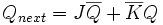
If the T input is high, the T flip-flop changes state ("toggles") whenever the clock input is strobed. If the T input is low, the flip-flop holds the previous value. This behavior is described by the characteristic equation:
 (or, without benefit of the XOR operator, the equivalent:
  )
)
and can be described in a truth table:
| T | Q | Qnext | Comment |
|---|---|---|---|
| 0 | 0 | 0 | hold state(no clk) |
| 0 | 1 | 1 | hold state(no clk) |
| 1 | 0 | 1 | toggle |
| 1 | 1 | 0 | toggle |


A toggle flip-flop composed of a single RS flip-flop that becomes an oscillator, when it is clocked. To achieve toggling, the clock pulse must have exactly the length of half a cycle. While such a pulse generator can be built, a toggle flip-flop composed of two RS flip-flops is the easy solution. Thus the toggle flip-flop divides the clock frequency by 2 ie. if clock frequency is 4 MHz, the output frequency obtained from the flip-flop will be 2 MHz. This 'divide by' feature has application in various types of digital counters.
A T flip-flop can also be built using a JK flip-flop (J & K pins are connected together and act as T) or D flip-flop (T input and Qprevious is connected to the D input through a XOR gates).
JK flip-flop

The JK flip-flop augments the behavior of the SR flip-flop by interpreting the S = R = 1 condition as a "flip" or toggle command. Specifically, the combination J = 1, K = 0 is a command to set the flip-flop; the combination J = 0, K = 1 is a command to reset the flip-flop; and the combination J = K = 1 is a command to toggle the flip-flop, i.e., change its output to the logical complement of its current value. Setting J = K = 0 does NOT result in a D flip-flop, but rather, will hold the current state. To synthesize a D flip-flop, simply set K equal to the complement of J. The JK flip-flop is therefore a universal flip-flop, because it can be configured to work as an SR flip-flop, a D flip-flop or a T flip-flop.
The characteristic equation of the JK flip-flop is:
and the corresponding truth table is:
| J | K | Qnext | Comment |
| 0 | 0 |  | hold state |
| 0 | 1 |  | reset |
| 1 | 0 |  | set |
| 1 | 1 |  | toggle |
D flip-flop

The Q output always takes on the state of the D input at the moment of a rising clock edge, and never at any other time. [4] It is called the D flip-flop for this reason, since the output takes the value of the D input or Data input, and Delays it by one clock count. The D flip-flop can be interpreted as a primitive memory cell, zero-order hold, or delay line.
Truth table:
-
-
Clock D Q Qprev Rising edge 0 0 X Rising edge 1 1 X Non-Rising X constant
-
('X' denotes a Don't care condition, meaning the signal is irrelevant)
These flip flops are very useful, as they form the basis for shift registers, which are an essential part of many electronic devices. The advantage of the D flip-flop over the D-type latch is that it "captures" the signal at the moment the clock goes high, and subsequent changes of the data line do not influence Q until the next rising clock edge. An exception is that some flip-flops have a 'reset' signal input, which will reset Q (to zero), and may be either asynchronous or synchronous with the clock.
Edge-triggered D flip-flop
A more efficient way to make a D flip-flop is not as easy to understand, but it works the same way. While the master-slave D flip flop is also triggered on the edge of a clock, its components are each triggered by clock levels. The "edge-triggered D flip flop" does not have the master slave properties.

A positive-edge-triggered D flip-flop.
Some of the flip flop IC numbers
| Manufacturer Part Number | MC10EL31DTR2G | |||
| Description | IC FLIP FLOP SET/RST ECL 8-TSSOP |
| Digi-Key Part Number | NL17SZ74USOSTR-ND | |||
| Manufacturer Part Number | NL17SZ74US | |||
| Description | IC FLIP FLOP SGL D-TYPE LOG US88 |
C FLIP FLOP/CLOCK DRIVER 14-DIP - N74F5074N
| Digi-Key Part Number | 568-3180-5-ND | |||
| Manufacturer Part Number | N74F5074N | |||
| Description | IC FLIP FLOP/CLOCK DRIVER 14-DIP |
A CIRCUIT DIAGRAM SHOWING
MASTER AND SLAVE SECTION
Master-slave D flip-flop
A master-slave D flip-flop is created by connecting two gated D latches in series, and invert the enable input to one of them. It is called master-slave because the second latch in the series only changes in response to a change in the first (master) latch.

For a positive-edge triggered master-slave D flip-flop, when the clock signal is low (logical 0) the “enable” seen by the first or “master” D latch (the inverted clock signal) is high (logical 1). This allows the “master” latch to store the input value when the clock signal transitions from low to high. As the clock signal goes high (0 to 1) the inverted “enable” of the first latch goes low (1 to 0) and the value seen at the input to the master latch is “locked”. Nearly simultaneously, the twice inverted “enable” of the second or “slave” D latch transitions from low to high (0 to 1) with the clock signal. This allows the signal captured at the rising edge of the clock by the now “locked” master latch to pass through the “slave” latch. When the clock signal returns to low (1 to 0), the output of the "slave" latch is "locked", and the value seen at the last rising edge of the clock is held while the “master” latch begins to accept new values in preparation for the next rising clock edge.

By removing the left-most inverter in the above circuit, a D-type flip flop that strobes on the falling edge of a clock signal can be obtained. This has a truth table like this:
-
-
D Q > Qnext 0 X Falling 0 1 X Falling 1
-
Most D-type flip-flops in ICs have the capability to be set and reset, much like an SR flip-flop. Usually, the illegal S = R = 1 condition is resolved in D-type flip-flops.
-
-
Inputs Outputs S R D > Q Q' 0 1 X X 0 1 1 0 X X 1 0 1 1 X X 1 1
-
By setting S = R = 0, the flip-flop can be used as described above.
References
http://parts.digikey.com/1/parts/index10445.html?p=no-cache
http://en.wikipedia.org/wiki/Flip-flop_%28electronics%29
No comments:
Post a Comment